Comp 103 -- Lab
1
HSPICE Tutorial and PMOS Characteristics
Due: 09/23/2003
Goals of the assignment: To acquire initial proficiency in running
HSPICE, we will run simulations to plot the I-V characteristics of PMOS device.
Background Reading: See Rabaey, Sections 2.3, and 3.2.
Resources: HSPICE is available on the
suns. To use it, type "use hspice"
which sets up your permissions correctly to access the HSPICE tools. If you wish, you can put this line in your
.cshrc file so that it happens automatically whenever you start anew
shell. The first part of the labs is a
short tutorial on using HSPICE.
Part I. SPICE Tutorial:
Simple RC circuit
SPICE is the industry standard for circuit simulation. HSPICE is the Avant! version. The graphical user interface is called awaves.
SPICE simulates a circuit by defining all the nodes, and the circuit elements between the nodes.
Editing an Input file
SPICE files contain a number of sections:
title line
the first line of the file is always interpreted as the title
comments
lines that begin with * or $
netlist declaration
a list of the devices in the circuit, with each device specifying node connections at terminals
subcircuit definitions
a mechanism for expressing hierarchy in the circuit
device model definitions
voltage and current sources and associated waveforms
pulses, piecewise linear waveforms ,sinusoids
simulation control commands
what kind of simulation: DC, transient, AC
simulation output format commands
which node voltages or branch currents to print, and in what format
the last line is always .END
Naming Devices
The type of many elements are defined by the first letter of their name in the input file. To model a device you add a line to the netlist where the first word is the name of the device. The name should start with the appropriate letter for the type of device you’re representing. The “xxx” represents any name you choose for your device.
Rxxx for resistor in Ohms
Lxxx for inductor in Henries
Cxxx for capacitor in Farads
Vxxx for voltage source in Volts
Ixxx for current source in Amperes
Mxxx for MOSFET devices (more on this later)
A VERY Simple Example
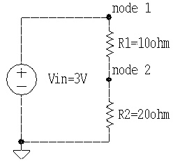
The corresponding input file for this circuit is:
* sample circuit
Vin 1 0 3
R1 1 2 10
R2 2 0 20
.END
if you use your favorite text editor to save this as a .spfile, you can simulate the circuit.
The netlist entries for 2 terminal devices begin with a word, followed by 3 numbers. The first two numbers are the nodes the terminals are attached to. The third number is the value of the device. For the previous example both resistors were in ohms. The default unit for a resistor is ohms. If the circuit had resistors of 10 mOhms you would represent that as“10 m” in the netlist.
Running HSPICE
To run HSPICE type:
hspice inputfile > outputfile &
Where
inputfile is the name of the .sp file you want to simulate and
outputfile is the name of the file you want to store the SPICE text output
If outputfile is omitted then the output is sent to stdout.
If the & is omitted the job is run in foreground mode
Unix Hint: in case you forget the & you can toggle back and forth between the foreground and the background by pressing
> ^ Z (control –Z)
>bg
this places the process into the background
Models
In SPICE you can define many parameters about a type of device, and then instantiate many of these devices in your circuit. There are two kinds of parameters for circuit devices: design parameters and process parameters. Design parameters include length, width, and value of the device. Process parameters define characteristics about the material and how it was made. Transistors have many process parameters and can be very individualized. SPICE requires that these parameters be defined before you can use a transistor in your circuit. Other elements, like resistors, are more standardized and SPICE allows the process parameters to be neglected. The only applicable parameter is the resistivity, which is given in the netlist when the device is instantiated.
Follow this link to the process parameters for the NMOS and PMOS transistors we are using. Include a model definition at the beginning of a .sp file before instantiating any transistors.
Part II. Advanced SPICE
Tutorial -- Simulating an NMOS Transistor
a) Copy the following SPICE code and save it as a .sp file.
*NMOS Transistor Simulating in HSPICE
* Model Section
.MODEL NMODEL NMOS
+ LEVEL =3 THETA =0.3873 VTO =0.76 UO =515
+ GAMMA =0.5 PHI =0.78 TOX =1.5e-08 NSUB =8.623e+16
+ XJ =2.5e-07 LD =1e-07 DELTA =0 VMAX =219900
+ NFS =1e+10 JS =5e-07 CJ =0.000318 CJSW =3.85e-10
+ MJ =0.5 MJSW =0.26 PB =0.75 CGSO =2e-10
+ CGDO =2e-10 CGBO =0 KAPPA =0.4624 ETA =0.008652
* The Netlist
* transistor_name=M1 drain_connection=d, gate_connection=g,src_connection = 0
* Bulk_connection = 0 Model=NMODEL
M1 d g 0 0 NMODEL L=2u w=10u
Vds d 0
Vgs g 0 DC 5 *the DC can be implied or stated explicitly
* The analysis
** sweep both Vds from 0 to 5 volts in increments of .2, and Vgs from 0 to 5 volts in increments of 1
.DC Vds 0 5 0.2 Vgs 0 5 1
** Plot the current value through the transistor
.plot DC I(M1)
** Need this to make right data for awaves
.option POST brief
.end
There are three main sections in this file:
* The models used. A model in SPICE is a description of the parameters of the equations used by SPICE to analyze the circuit.
* The netlist description. Netlist is the representation of all circuit elements and their connectivity. The transistor here is named M1. The length of M1 is defined as 2 micro meters.
* The analysis to be performed during the simulation. We are requesting a the DC Transfer characteristic of the circuit that would
allow us to plot IDS = f(VDS, VGS) of an NMOS device.
b) Simulate the circuit netlist.
hspice NMOS.sp > NMOS.out
Upon proper completion you should read something like...
>info: ***** hspice job concluded
real 0.5
user 0.1
sys 0.1
c) Definition of Output Files
NMOS.sp is the input netlist. (your file)
NMOS.sw0 is the DC sweep data output. (used by awaves)
NMOS.tr0 is the transient data output. (used by awaves during transient analysis)
NMOS.out is the output listing from the HSPICE run. (look here for errors or text output about the circuit)
NMOS.st0 is the simulation run information. (not useful)
NMOS.ic is the information about the input to HSPICE. (not useful)
d) View the result of the DC Analysis
Let's examine the DC analysis:
> awaves &
This will load Awaves.
Once Awaves loads, click on Design and select Open. This will bring up a menu to select which HSPICE netlist file you want to display.
Your netlist NMOS.sp should be listed, if not, you might have to change to the right directory using the directory tab above or set the
FILTER option to view "all files". Once you have found your directory, double click on NMOS.sp. You should now be looking at the
Results Browser.
To view the DC characteristics, click on DC: nmos IV characteristics. In the two small option boxes below: Select Current Type,
and double click on the I(m1) Curve.
e) Add labels for VGS=1, ... VGS=5 [Panel menu, Add label],and then Print the waveform for I(m1): [Tools menu, Print]. Make
sure to click the time and date option. If you' output is blank, try flipping the colors via [Window menu, Flip Color].
Part III.
Voltage-Transfer Characteristics for a PMOS device.
a) Replace the NMOS device in NMOS.ps with a PMOS device. Make the PMOS device W/L = 20/2.
b) Modify Vds and Vgs and the bulk bias to allow you to examine the interesting part of the PMOS operation. & make sure the bulk
is tied to a constant VDD src.
c) Run HSPICE and Awaves, and
d) Plot the wave form that shows the current of the PMOS vs. the drain to source voltage.
What should be turned in:
Turn in your .sp file for the PMOS, and also a plot of the waveform that shows the current of the PMOS vs. the drain to source voltage.
Make sure all your plots have the time and date stamp, and are annotated with useful data.
References
http://www.eeap.aston.ac.uk/eeap/documents/user-guides/hspice.html
http://www.ee.washington.edu/class/cadta/hspice/
http://www.ee.ed.ac.uk/~dar/ee4-vlsi/L1-runsim.html